Semiconductor Superlattices and Superstructures
Superlattices and superstructures refer to 1D/2D periodic stacks and structures blending two or more materials. In our group, we aim to develop process and materials yielding superlattices or superstructures containing optoelectronic nanomaterials, organic semiconductors, dielectrics, and plasmonic materials. Through tunning the superstructure lattice parameters, we aim to control multiscale physical mechanisms ranging from spontaneous emission, energy transfer, to subwavelength refraction and interference.
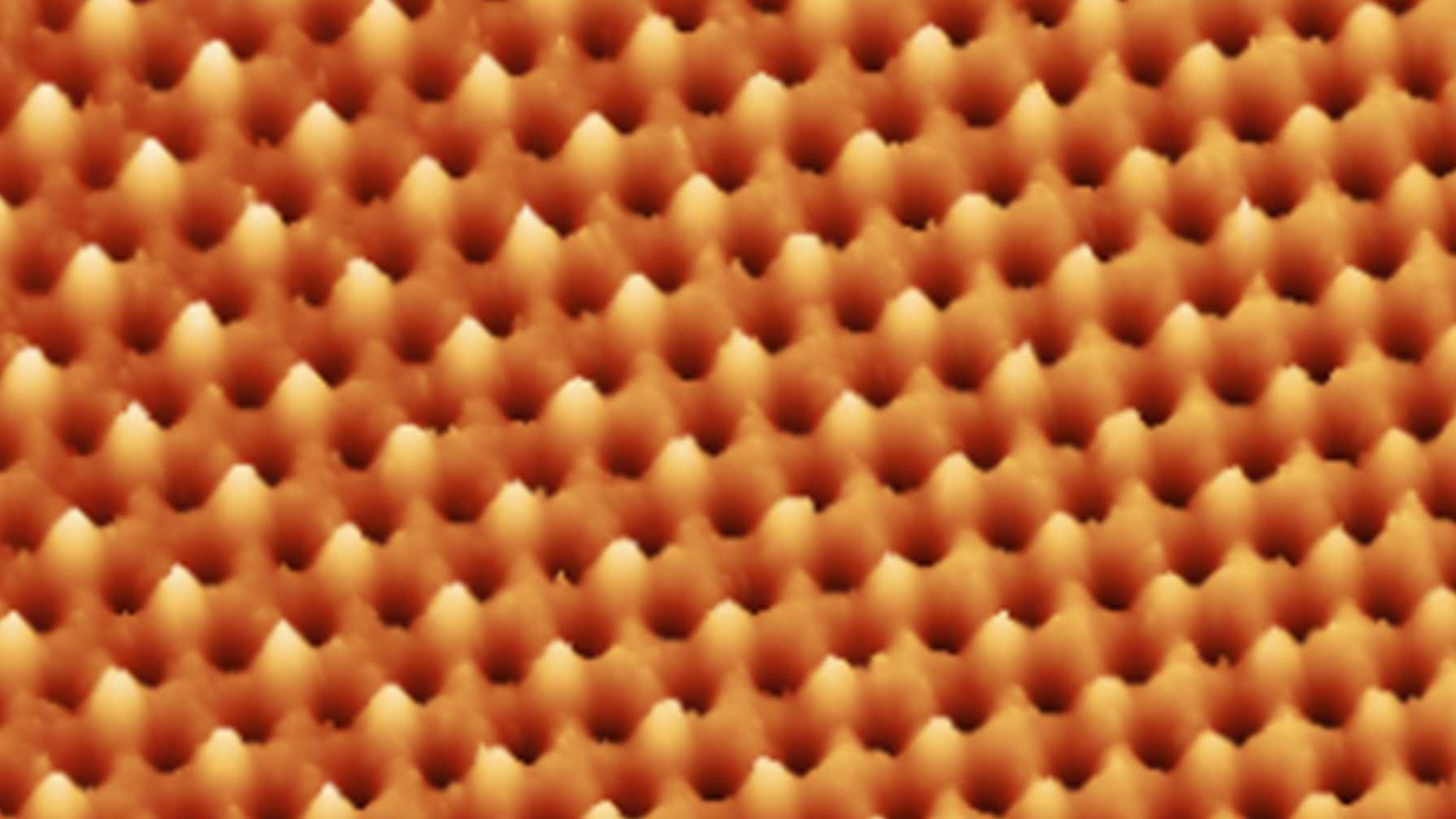
For example, in 2025, we announced a direct nanopatterning technology - the molecular-beam holographic lithography (MBHL), for the fabrication of complex 3D surfaces and self-aligned superstructures made by any evaporable materials, such as metals, oxides, and organic semiconductors, with the lateral critical dimension down to 50 nm. The technology enabled the first scalable process for the fabrication of nanoscale organic light emitting diodes (Nano-OLEDs), with periodicity and lateral dimension at scales of 250 and ~100 nm, respectively.
Key Publications:
- Sci. Adv. 3 (12), eaaq0208, (2017). external page link
- Nat. Commun. 11, 387 (2020). external page link
- ACS Nano 16(11), 18459 (2022). external page link
- Nat. Commun. 16, 3436 (2025). external page link
- Nat. Photonics 20, --- (2026). external page link